Electrical Double Layer based devices, College of Engineering
By A Mystery Man Writer
Description
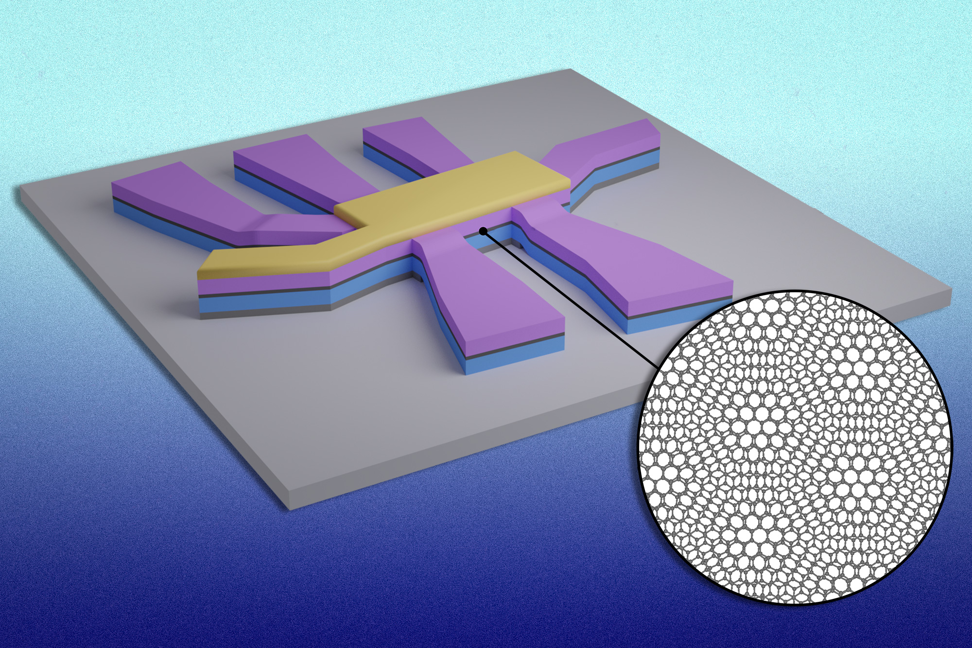
Immersing a metal (electrode) in a salt solution will spontaneously accumulate ions due to image charge to form the well known electrical double layer (EDL). Sign of the charge depends on the Fermi level (i.e., the electrochemical potential) difference between the metal and the solution. For example, gold will accumulate negative ions (i.e., anions). The interfacial structure

Rabbit reimagines the digital experience with AI-powered R1 device

Routing Requirements for a USB Interface on a 2-Layer PCB, Blog
Electrical double layer theory

PDF) Laboratory Verification of Electric Double Layer Capacitor Based Power System for a Simple CubeSat Mission

Smart supercapacitors from materials to devices - Wang - 2020 - InfoMat - Wiley Online Library
Lecture 22: Electrical Double Layer (EDL)

Frontiers Discernment on assistive technology for the care and support requirements of older adults and differently-abled individuals
Study: Superconductivity switches on and off in “magic-angle” graphene, MIT News

What is a PCB and PCB Design?
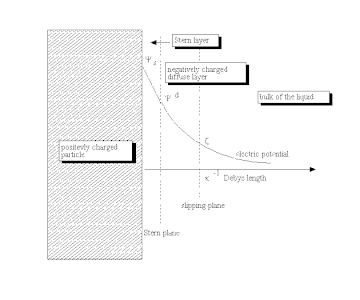
Double layer (surface science) - Wikipedia

Multi-layer Red Team vs. Blue Team Methods towards Secure Cyber-Physical Energy Systems, CEMSE
from
per adult (price varies by group size)